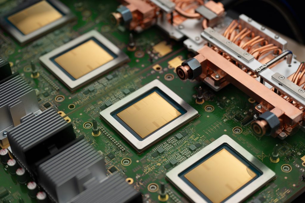
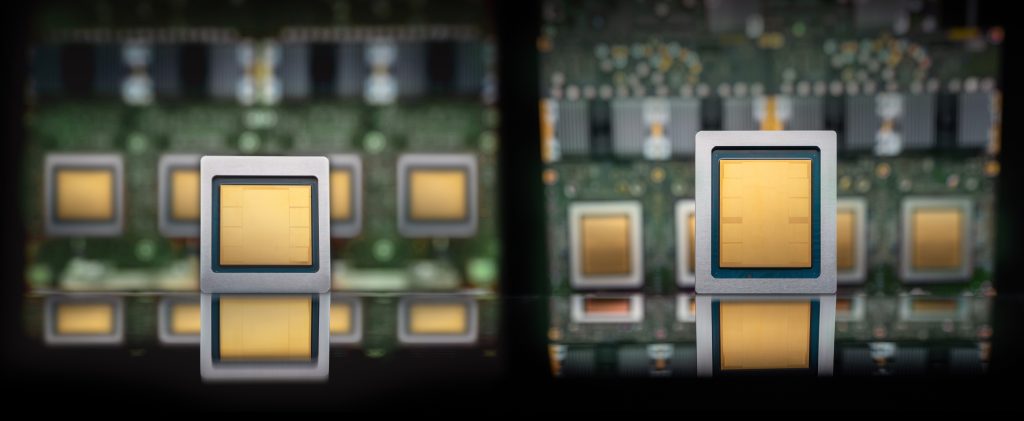
For most of Google’s Tensor Processing Unit’s (TPU) decade-long history, Google has shipped a single chip per generation — sometimes with variations in its SKUs but based on the same architecture. That same architecture was tasked with pre-training frontier models and running inference on them. Now, Google believes it’s time to change that as those two modes are diverging.
At Google Cloud Next on Wednesday, the company introduced TPU 8t and TPU 8i, two distinct chips designed for training and inference. Google’s argument is that agentic workloads have made it impossible for a single accelerator to be optimal at both, so the only way to keep improving price-performance at the frontier is to stop trying.
Two chips, one family
TPU 8t keeps the 3D torus interconnect, a network topology that wires the chips into a three-dimensional grid in which each dimension wraps around like a ring, giving every chip direct links to its six nearest neighbors. It also keeps Google’s standard SparseCores to accelerate the irregular memory-access patterns of embedding lookups.
TPU 8i replaces those SparseCores with a new on-die Collectives Acceleration Engine, which Google says cuts the latency of global synchronization operations — the work that dominates chain-of-thought decoding and Mixture-of-Experts routing — by up to 5 times. The network topology changes, too.
Google’s argument is that agentic workloads have made it impossible for a single accelerator to be optimal at both, so the only way to keep improving price-performance at the frontier is to stop trying.
TPU 8i abandons the 3D torus for a new Dragonfly-inspired layout called Boardfly: a hierarchical topology that fully connects the chips within small groups, then links the groups to one another with direct optical long-haul cables rather than routing traffic through a grid. Where a torus is built for neighbor-to-neighbor communication, a Dragonfly is built for short paths between any two chips in the system. Google says the new layout cuts the maximum hop count for a 1,024-chip pod from 16 to 7.
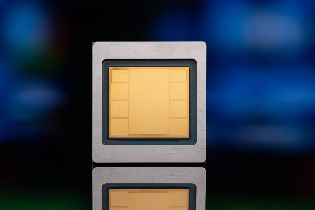
The single most important thing to say about TPU 8i is that Google designed it to break the memory wall. The chip triples on-chip SRAM to 384 MB and pushes the HBM capacity to 288 GB. That’s enough, Google says, for the key-value cache of a long-context reasoning model to live entirely on silicon.
For agentic workflows, every off-chip memory access incurs latency in a user-facing response and compounds across reasoning turns. Keeping the working set on-chip is the whole ballgame.
That’s why TPU 8i has higher per-chip bandwidth than TPU 8t, which may seem counterintuitive if you still think of training as the harder workload. Training is compute-bound while agentic inference is memory-bound.
Why now?
A year ago, Google essentially argued the split wasn’t needed. When the company launched Ironwood — the seventh-generation TPU, which remains its flagship in general availability — it marketed the chip as “the first Google TPU for the age of inference.” It pitched the same silicon for pre-training, training, and large-scale serving.
But training and inference have always had somewhat different demands. What changed over the last year is that inference itself changed. Traditional inference from early chatbot-like systems — one prompt, one response — is one workload. But agentic inference, with a primary agent that decomposes a goal into subtasks and dispatches them to a fleet of specialized agents that reason in long loops, is a very different one. It puts much heavier pressure on key-value (KV) cache size, all-to-all collectives, and tail latency.
Models, too, have changed, with a stronger focus on Mixture-of-Experts systems — another area where high memory bandwidth is beneficial.
The training workload hasn’t stood still either. Frontier models now require clusters in the hundreds of thousands of chips to converge on reasonable timelines. A TPU 8t superpod scales to 9,600 chips, and Google says its new Virgo data center fabric and Pathways software can stitch more than a million TPU 8t chips into a single logical training cluster.
Google claims TPU 8t delivers roughly 2.7 times better price-performance than Ironwood for training, and that TPU 8i delivers 80 percent better price-performance for inference. Whether those numbers hold up in customer benchmarks is a different question.
The opposite bet from AWS
The bifurcation reads very differently when set against what AWS has been doing. At re:Invent 2025, Amazon shipped Trainium3 and made it clear that the chip would handle both training and inference. The Inferentia line has effectively been wound down. The AWS argument is that inference is becoming more like training as models get larger and reasoning chains get longer, and that the gap between training-optimized and inference-optimized silicon is closing rather than widening.
Google’s eighth-generation TPU is a public bet against that thesis.
Nvidia occupies the middle ground. Vera Rubin NVL72, the platform Google is reselling through its new A5X bare-metal instances, is a single rack that does both training and inference. Per chip, Nvidia’s Rubin GPU is much more powerful than either TPU 8 variant, with roughly 50 PFlops of NVFP4 inference per GPU versus 10.1 FP4 PFlops per TPU 8i chip. Per pod, the math inverts: an NVL72 rack tops out near 3.6 ExaFlops of NVFP4 inference, while a TPU 8i pod hits 11.6 ExaFlops of FP8 across 1,152 chips.
The two companies are trying to achieve similar results but have different philosophies: fewer, beefier chips on NVLink for Nvidia; many smaller chips on a custom fabric for Google.
What customers actually get
Both chips ship later this year, with GA timing unspecified, through Google’s AI Hypercomputer architecture.
Two pieces of the customer story matter more than the keynote framing suggested. TPU 8t and 8i are the first TPUs to offer bare-metal access, meaning customers can manage the host themselves rather than going through Google’s VM layer. That is a concession to a class of workloads — low-level kernel development, latency-sensitive inference, third-party ISVs — that have historically picked Nvidia by default.
Native PyTorch on TPU, which Google is calling TorchTPU, is now in preview. JAX has always been a first-class framework on TPU, and PyTorch support has been awkward for as long as TPUs have been sold to external customers. If TorchTPU works in production, it removes one of the longest-standing reasons developers default to GPU infrastructure.
Goodput, not just FLOPs
At training scales of 10,000 or more chips, the gap between peak FLOPs and actually useful FLOPs can be enormous. A single stalled chip can throttle a synchronous job, and every checkpoint restart is time the cluster is not training.
The bet inside Google seems to be that the agentic era won’t reward a single general-purpose accelerator the way the pretraining era did.
Google says TPU 8t targets 97 percent “goodput,” its term for the share of provisioned compute doing productive work. ‘Goodput’ is not a term that’s easy to love, but Google seems keen on using it.
The bet inside Google seems to be that the agentic era won’t reward a single general-purpose accelerator the way the pretraining era did.
Also on the hardware roadmap
The eighth-generation TPUs are the headline, but they are part of a broader infrastructure refresh.
Google also announced A5X bare-metal instances on NVIDIA Vera Rubin NVL72; Axion N4A, a new Arm-based VM family on Google’s custom CPU (now the host across TPU 8t, TPU 8i and N4A, making Axion a structural answer to Nvidia’s Grace and Vera); the Virgo Network fabric, which can connect 134,000 TPU 8t chips at 47 Pb/s of bisectional bandwidth; Managed Lustre at 10 TB/s and 80 PB, and Rapid Buckets on Cloud Storage with sub-millisecond latency for checkpoint work; Z4M VMs with 168 TiB of local SSD for ISV-built parallel file systems; and GKE updates that include an Inference Gateway with machine-learning-driven, latency-aware routing.
All of these are meant to work together seamlessly. Virgo’s bandwidth targets were sized around TPU 8t’s parallelism requirements. A dedicated KV cache storage subsystem was sized around TPU 8i’s on-chip footprint. Axion’s topology was tuned to remove the TPU host bottleneck.
The post Google splits its TPU line in two for the agentic era appeared first on The New Stack.